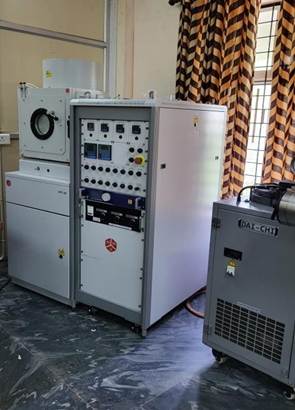
Booking Details

RF Sputtering


Name of the equipment:

RF Sputtering


Make & Model:

HIND HIGH VACUUM AUTO 500, D1307


I-Stem Registration ID-

………………………                       


Category of Instrument

Sample Preparation


Types of Analysis / Testing

Sample Preparation


Application:

1. Coating (Thin Films)

2. Semiconductor Industries

3. Biological / Polymer sample coating


Description of Instrument

RF sputtering is a physical vapor deposition (PVD) technique used to deposit thin films. It involves bombarding a target material with energetic ions, which then dislodge atoms that deposit on a substrate to form a thin film. RF sputtering utilizes radio frequency (RF) power to create and maintain a plasma, accelerating ions that impact the target


Book through I-STEM:

https://www.istem.gov.in/


Slot Booking Link

I-STEM Slot Booking link for External User


Booking available for

Internal and External Both


Requisition form for

Internal

External


Faculty In-charge:

Dr. Soney Varghese


Email ID:

soneyva@nitc.ac.in


Phone number:

 +91-9446792019

Contact Details


Technical Staff:

Anurag C (ST)

anuragc@nitc.ac.in


Department

MSED


Office Email ID

msedoffice@nitc.ac.in


Location

Room No. 101, Department of Materials Science and Engineering


Lab Phone No

0495-2286528

Features, Working Principle and Specifications Type of Sample Required for Analysis / Testing (Quantity, Pre-Preparation, State etc.) Guidelines for Sample Submission – User Instructions


Features of the equipment


Ø  RF (Radio Frequency) sputtering is a physical vapour deposition (PVD) technique used to deposit thin films by bombarding a target material with ions in a vacuum environment. It utilizes an alternating current (AC) power source at a radio frequency, typically 13.56 MHz, to create a plasma that accelerates ions to the target


Unique features/Measurement capabilities, if any

Instrument Technical Description and Major Specifications (This Specifications Limited to Major 5)


1.  To identify Topography

2.  To identify I/V Spectroscopy

3.  To identify F-D Spectroscopy

4.  To identify Nano Indentation

Measurement/Sample specifications:

·         Maximum Size

·         2cm×2cm Film/Coated samples

·         No Liquid/Powder samples


User Charges Rs. (GST Extra) 


Ø  Login to the ISTEM portal and book the slot.

Ø  Samples can be sent in the address,

Department of Materials Science and Engineering,

NIT Calicut,

NIT Campus PO-673601

                  Calicut, Kerala.


Internal

External Academic Institutes

National R&D Lab

Industry

1.Coating

(Thin Films)

2.Semiconduct

or Industries

3.Biological /

Polymer

sample coating

500/hour +

Target charges

1000/hour +

  Target charges

1000/hour +

  Target charges

2000/hour +

  Target charges